
Photolithography is essential in semiconductor manufacturing, enabling the creation of intricate patterns on silicon wafers. These patterns are the foundation of integrated circuits and microchips, which power our modern devices. This article explains the photolithography process, its variations, and its significance in technology development.
Key Takeaways
- Photolithography is essential in semiconductor manufacturing, enabling the precise creation of patterns on silicon wafers for integrated circuits and other electronic components.
- The technique involves various types of photolithography, such as UV, DUV, and EUV, each providing different resolution and feature size capabilities, crucial for advancing microfabrication.
- Challenges in photolithography include high equipment costs, cleanroom requirements, and limitations due to light diffraction, which necessitate ongoing innovations and alternative techniques for future improvements.
Understanding Photolithography: Techniques, Uses, and Benefits
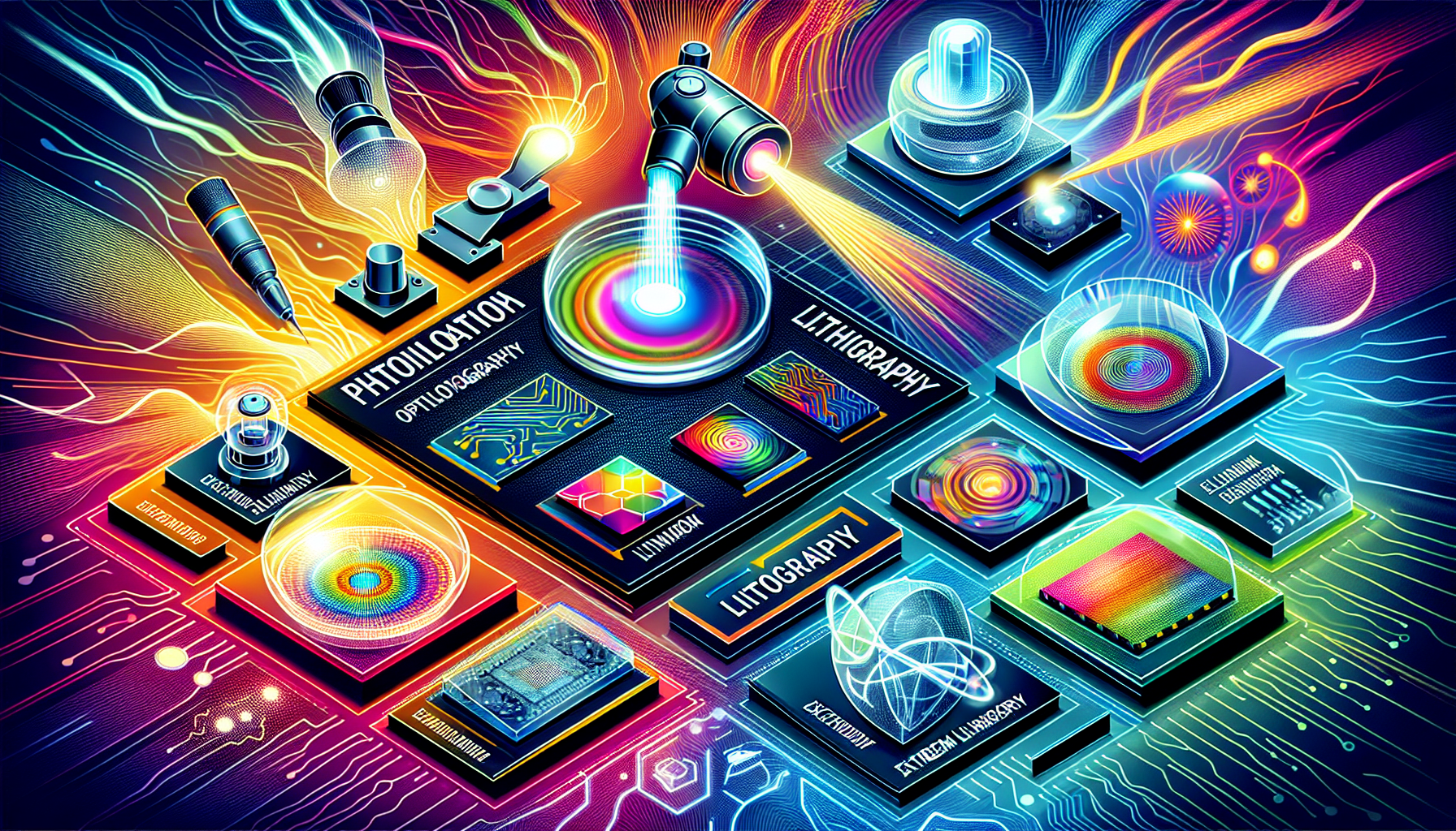
Photolithography is a sophisticated technique used to create precise patterns on silicon wafers through the application of photoresist and ultraviolet (UV) light. This method is indispensable in the production of integrated circuits, transistors, and printed circuit boards, which form the foundation of modern electronics. Photolithography has significantly impacted semiconductor manufacturing by enabling the creation of smaller and more advanced electronic devices.
The photolithography process includes applying a photosensitive material called photoresist, exposing it to light through a mask, and developing the pattern. Various types of photolithography, such as ultraviolet (UV), extreme ultraviolet (EUV), and deep ultraviolet (DUV), each offer different feature size capabilities, further expanding the possibilities for innovation.
Photolithography is crucial for creating the intricate patterns required for the next generation of electronic devices.
Introduction
Photolithography is a pivotal technique in semiconductor manufacturing, utilized to transfer precise patterns onto substrates through the strategic application of light. This process is critical for the creation of integrated circuits and microchips, which are the building blocks of all modern electronic devices.
Photolithography is also used in fields like microelectromechanical systems (MEMS) and biotechnology, highlighting its versatility and importance. Professionals in these industries must thoroughly understand photolithography, as it underpins much of the technology that powers our world.
Basics of Photolithography
Photolithography uses light to transfer a pattern onto a substrate coated with a photosensitive material, known as photoresist. The process involves applying photoresist, exposing it to light through a mask, and developing the pattern.
Types of photolithography like ultraviolet (UV), deep ultraviolet (DUV), and extreme ultraviolet (EUV) lithography offer unique capabilities in feature size and resolution. This technique is fundamental to the creation of integrated circuits and microprocessors, making it a cornerstone of modern semiconductor manufacturing.
Photolithographic Process
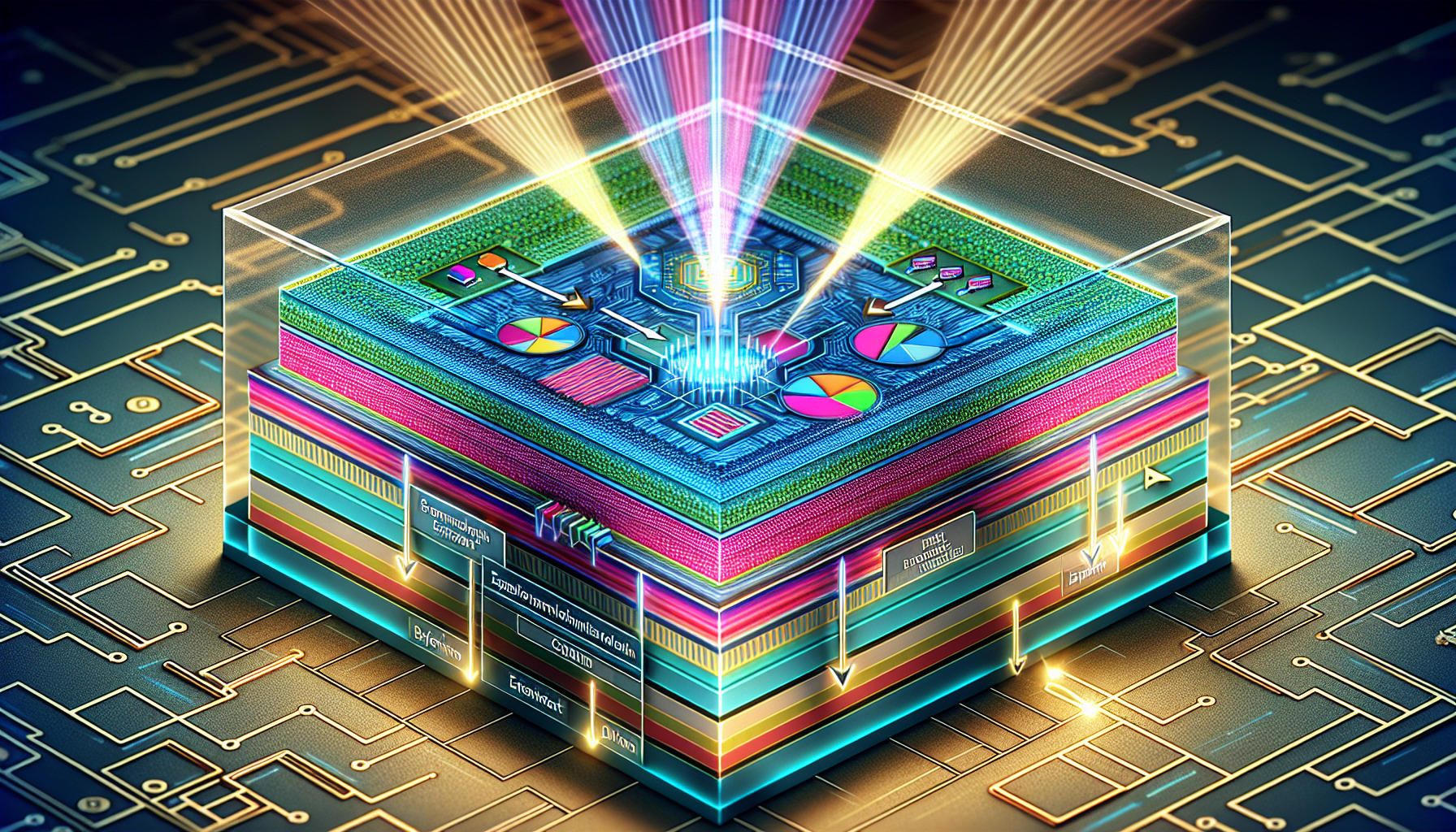
The photolithographic process meticulously creates precise patterns on a silicon wafer. It begins with the thorough cleaning of the substrate to remove any contaminants that could interfere with the process. Following this, a layer of photoresist is applied to the substrate, which is then baked to remove solvents and enhance adhesion. This preparation ensures a uniform, stable surface for the light exposure.
During the exposure phase, high-intensity UV light is directed through a photomask, which contains the desired pattern. The light chemically changes the photoresist, altering its solubility in exposed areas. This step defines the pattern for the next stage. After exposure, the wafer undergoes development where the altered photoresist is selectively dissolved, revealing the desired pattern.
The final steps include etching to transfer the pattern onto the substrate and stripping the remaining photoresist. Depending on the application, this may involve wet chemical etching or dry etching techniques. The precision of these steps ensures the integrity and functionality of the final electronic components.
Optical Lithography vs. Other Methods
Optical lithography, also known as photolithography, uses light to transfer patterns from a mask onto a photoresist-coated wafer. Its widespread use is due to its ability to produce high-resolution patterns efficiently. However, as the demand for smaller and more complex features grows, other methods such as electron beam lithography and extreme ultraviolet lithography (EUV) are gaining prominence.
Electron beam lithography offers finer resolution by using focused electron beams instead of light, suitable for very small features. EUV lithography, implemented in mass production by companies like Samsung since 2018, utilizes extremely short wavelengths of light to achieve unprecedented resolution and feature sizes.
Nanoimprint lithography is another emerging technique that creates intricate patterns at a lower cost compared to optical lithography. These advancements are critical as they push the boundaries of what is possible, enabling the continued miniaturization and enhancement of electronic devices.
Photoresists in Photolithography
Photoresists are light-sensitive materials in photolithography, enabling the creation of detailed patterns on substrates. Applied to a silicon wafer, these materials undergo chemical changes when exposed to light, forming the basis for pattern development.
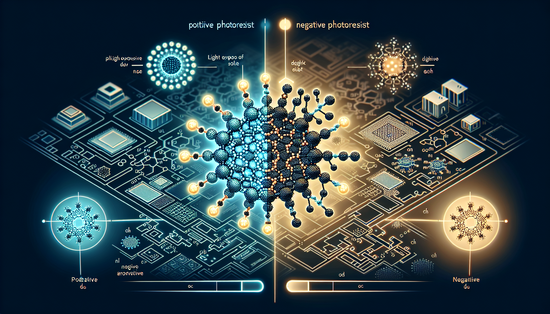
Positive and Negative Photoresists
Photolithography uses two primary types of photoresists: positive and negative. Positive photoresists become soluble in exposed areas after UV exposure, allowing selective removal during development. This type of resist is particularly useful for creating fine details and intricate patterns where precision is crucial.
Negative photoresist hardens and becomes insoluble where light hits, enabling high-aspect-ratio features. Both types of photoresists are vital, with applications varying based on their chemical properties and desired features.
Photoresist Coating Techniques
Photoresist is typically applied using spin coating. This method achieves a uniform layer of photoresist, essential for optimal pattern transfer. During spin coating, the wafer rotates at high speeds, spreading the photoresist evenly.
The photoresist layer thickness can vary from 0.1 to 10 micrometers, depending on fabrication requirements, and the resist layer thickness can also play a crucial role.
Exposure Systems and Techniques
Exposure systems in photolithography play a crucial role in transferring intricate patterns from a photomask onto a photoresist-coated wafer. These systems use optical setups to project light accurately onto the wafer, creating precise patterns.
The choice of exposure system and technique impacts the resolution and quality of the final patterns.
Mask Alignment and Pattern Transfer
Mask alignment and pattern transfer are critical in photolithography. Three primary methods transfer mask patterns onto a wafer: direct contact, proximity, and projection exposure. Each of these methods has its own set of advantages and challenges. In contact and proximity lithography, the mask must align precisely with existing wafer features, and light intensity must be uniform to ensure accurate pattern transfer.
A mask aligner positions the photomask accurately over the substrate, ensuring the mask pattern is crucial for producing semiconductor devices with multiple layers that fit together perfectly. The precision of pattern transfer ensures the final product meets required specifications and performance standards.
Deep Ultraviolet (DUV) and Extreme Ultraviolet (EUV) Lithography
Deep ultraviolet (DUV) lithography uses ultraviolet light for high-resolution patterning, making it a staple in semiconductor manufacturing. Recent advancements in DUV technology have enabled the transfer of smaller features onto substrates, enhancing the overall efficiency and precision of the photolithography process. This technique remains key in producing advanced semiconductor devices.
Extreme ultraviolet (EUV) lithography is the cutting edge of photolithographic technology. Using shorter wavelengths of light, EUV lithography creates patterns with unprecedented precision and detail. Integrating artificial intelligence and machine learning into EUV systems has optimized the manufacturing process, improving adaptability and efficiency.
These advancements highlight the ongoing evolution of lithography technologies, pushing the boundaries of what is possible in semiconductor manufacturing.
Development and Etching Processes
Development and etching processes in photolithography define the desired features on the wafer surface. These processes require a cleanroom environment to prevent contaminants, ensuring the integrity and precision of the final product.
Wet and Dry Etching Techniques
Etching techniques in photolithography are broadly classified into wet and dry methods. Wet etching immerses the wafer in a chemical solution that selectively removes material from exposed areas. While less precise and prone to undercutting, it is used where high precision is not critical.
Dry etching employs gases instead of liquids, providing better resolution for small features and minimizing unintended undercutting. This technique is useful for creating intricate patterns with high precision, making it a preferred choice for many semiconductor manufacturing applications.
Post-Exposure Baking and Final Steps
Post-exposure baking hardens and strengthens the photoresist. This process reduces pattern distortion by allowing the photoresist to achieve greater stability before subsequent processing steps.
After photoresist development, the entire wafer undergoes a hard bake to enhance adhesion of the remaining resist to the substrate. Following this, additional processes such as wet or dry etching, selective metal deposition, and ion implantation are performed, completing the intricate fabrication of semiconductor devices.
Applications of Photolithography
Photolithography creates intricate patterns on silicon wafers, facilitating the manufacturing of integrated circuits, transistors, and other critical components in modern electronics. Its applications extend beyond semiconductors to include microstructures for sensors, MEMS devices, and biochips, showcasing its versatility.
This versatility underscores the importance of photolithography in various high-tech industries.
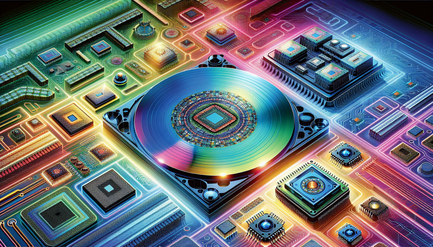
Semiconductor Manufacturing
In semiconductor manufacturing, photolithography is crucial for producing integrated circuits and other electronic components. The process enables the development of smaller and more efficient devices by creating precise patterns on silicon wafers. Extreme ultraviolet (EUV) lithography, which began mass production at Samsung in 2018, represents a significant advancement over traditional photolithography, offering enhanced resolution and feature sizes.
Photolithography is versatile, allowing for the patterning of various materials including glass, silicon, and flexible substrates. Patterns created in the photoresist can be used as masks for etching or metal deposition, typically achieved through dry etching techniques, highlighting its critical role in semiconductor fabrication.
Microelectromechanical Systems (MEMS)
Photolithography is instrumental in producing microelectromechanical systems (MEMS), including sensors, actuators, and other microstructures. These devices find applications in automotive, healthcare, and consumer electronics, where precise and reliable microstructures are essential.
The ability to create detailed patterns on silicon wafers enables the development of sophisticated MEMS devices integral to modern technology.
Biotechnology and Medical Diagnostics
In biotechnology and medical diagnostics, photolithography plays a crucial role in surface patterning and microfabrication. These techniques are essential for developing lab-on-a-chip devices, biosensors, and other diagnostic tools. Surface patterning studies contribute to new methods for manipulating and controlling liquid behaviors on solids, vital for various biotechnological applications.
This has significant implications for improving medical diagnostics and advancing healthcare technologies.
Advantages and Disadvantages of Photolithography
Photolithography offers high precision, scalability, and cost-effectiveness, making it a cornerstone of semiconductor manufacturing. However, it also presents challenges such as high equipment costs, the need for cleanroom environments, and limitations imposed by light diffraction limits.
Understanding these pros and cons is crucial for optimizing the process and pushing the boundaries of microfabrication.
Key Advantages
One of the main advantages of photolithography is its ability to create features as small as a few tens of nanometers, demonstrating its high precision capabilities. This precision is essential for producing the intricate patterns required in modern semiconductor devices. Additionally, photolithography is highly scalable, allowing for the patterning of various materials, including flexible substrates and glass, which broadens its application scope.
The use of deep ultraviolet (DUV) and extreme ultraviolet (EUV) lithography techniques significantly enhances resolution capabilities, enabling the creation of even smaller features in semiconductor devices. These advancements underscore the importance of photolithography in pushing the limits of microfabrication and supporting the ongoing miniaturization of electronic components.
Common Challenges
Photolithography is associated with several challenges, one of which is the high cost of equipment and the necessity of maintaining a cleanroom environment. These requirements can be prohibitively expensive for many manufacturers, limiting access to this advanced technology. Additionally, the resolution limit imposed by the diffraction of light restricts the smallest attainable feature size, posing a significant challenge for further miniaturization.
Other common challenges include controlling deformities, ensuring precise alignment, and maintaining consistency throughout the photolithography process. These issues can affect the quality and performance of the final product, making it essential to continually refine and optimize the process to meet the ever-increasing demands of the semiconductor industry.
Future Trends in Photolithography
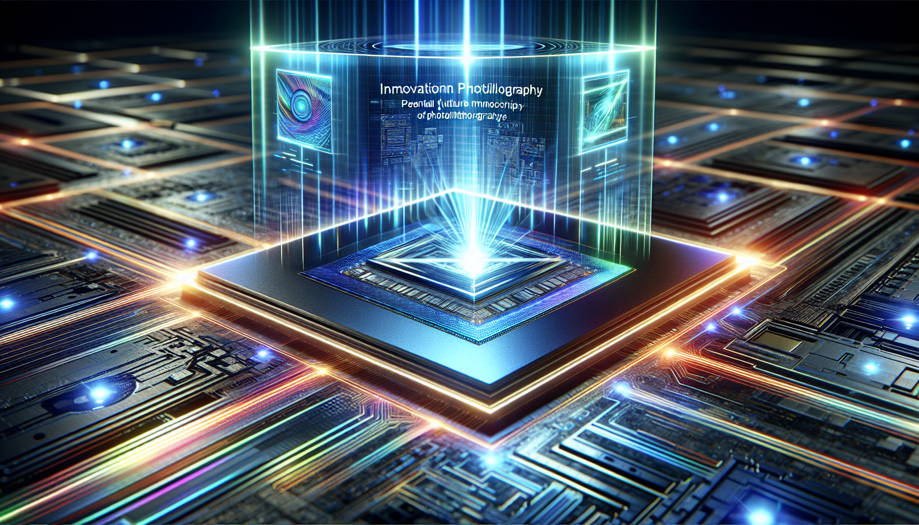
The future of photolithography is poised for exciting developments, driven by advancements in light sources, materials, and alternative techniques. Innovations in these areas are expected to enhance the precision, efficiency, and capabilities of photolithographic processes, supporting the ongoing evolution of semiconductor manufacturing and other high-tech industries.
Innovations in Light Sources and Materials
Recent developments in laser-based light sources are improving the efficiency and precision of photolithographic processes. These advancements enhance accuracy in pattern transfer, enabling the creation of even more intricate and precise patterns on silicon wafers. Additionally, new resist materials are being developed to optimize performance for next-generation photolithography applications. These materials offer better adhesion and resolution, which are crucial for advanced semiconductor manufacturing.
The continuous improvement of light sources and resist materials is essential for pushing the boundaries of what photolithography can achieve. These innovations will play a pivotal role in supporting the development of smaller, more powerful, and more efficient electronic devices, driving the next wave of technological advancements in the semiconductor industry.
Alternative Lithography Techniques
As the demand for higher resolution and lower production costs grows, alternative lithography techniques are gaining attention. Nanoimprint lithography, for example, offers the potential to create patterns with higher resolution than traditional methods, making it a promising alternative. This technique is being explored for its ability to produce intricate patterns at a lower cost and with higher throughput, which could revolutionize the fabrication process.
X-ray lithography is another emerging technique that holds promise for future semiconductor applications. Its ability to create smaller features and improve throughput makes it a viable alternative to current photolithographic methods. By leveraging shorter wavelengths of light, X-ray lithography can achieve higher resolution and precision, supporting the development of next-generation electronic devices.
Summary
Photolithography is an indispensable process in the modern technology landscape, enabling the creation of intricate patterns on silicon wafers that form the foundation of countless electronic devices. From its foundational steps involving photoresists and light exposure to advanced techniques like EUV lithography, photolithography continues to evolve and push the boundaries of what is possible in semiconductor manufacturing. Its applications span various fields, including semiconductor manufacturing, MEMS, and biotechnology, highlighting its versatility and importance.
As we look to the future, innovations in light sources, materials, and alternative techniques promise to further enhance the capabilities of photolithography. These advancements will enable the continued miniaturization and improvement of electronic devices, driving technological progress and shaping the future of the semiconductor industry. By understanding the intricacies of the photolithographic process and staying abreast of emerging trends, professionals in the field can harness the full potential of this transformative technology.
Frequently Asked Questions
What is photolithography and why is it important?
Photolithography is a crucial process that employs light to transfer patterns onto photosensitive substrates, enabling the production of complex designs on silicon wafers vital for semiconductor manufacturing. Its importance lies in its ability to facilitate the development of advanced electronic devices.
What are the main steps involved in the photolithographic process?
The photolithographic process primarily involves substrate cleaning, applying photoresist, exposing it to light through a mask, developing the pattern, etching, and finally stripping the remaining photoresist. Each step is crucial for achieving precise microfabrication results.
What are the differences between positive and negative photoresists?
Positive photoresists are soluble in the exposed areas after UV exposure, allowing for selective removal, whereas negative photoresists harden and become insoluble in those areas, enabling the creation of high-aspect-ratio features. This distinction is crucial for specific applications in photolithography.
How do DUV and EUV lithography differ from traditional optical lithography?
DUV and EUV lithography differ from traditional optical lithography by utilizing shorter wavelengths of light, enabling them to achieve higher resolution and finer feature sizes. This advancement in technology, particularly with EUV, allows for more precise fabrication in advanced semiconductor manufacturing.
What are some emerging alternative lithography techniques?
Emerging alternative lithography techniques such as nanoimprint lithography and X-ray lithography present opportunities for higher resolution and improved production efficiency, making them promising options for future applications. These methods leverage advanced technologies to create smaller features at reduced costs.


